Why Semiconductor Automation Is Exploding Right Now
The semiconductor industry is undergoing the largest expansion in its history. The CHIPS and Science Act has committed federal subsidies and incentives to domestic chip manufacturing, triggering a wave of new fabrication facility (fab) construction that has created an unprecedented demand for automation professionals. Intel is building two new fabs in Chandler, Arizona and a mega-site in New Albany, Ohio. TSMC is constructing fabs in Phoenix, Arizona. Samsung is building a fab in Taylor, Texas. GlobalFoundries is expanding in Malta, New York. Micron Technology is building a new fab complex in Clay, New York. Each of these facilities requires thousands of automation engineers and technicians to design, install, commission, and maintain the extraordinarily complex equipment that turns raw silicon wafers into finished chips.
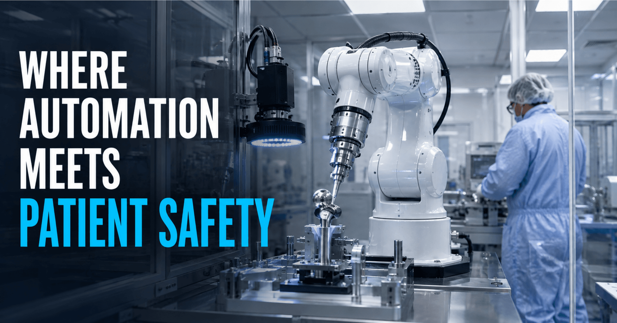
Semiconductor manufacturing is the most automation-intensive industry on the planet. A modern fab contains over 1,000 individual process tools, each controlled by sophisticated automation systems. Wafers move through 400 to 700 processing steps over a period of two to three months, handled entirely by automated material handling systems (AMHS) that transport wafer carriers between tools via overhead track systems and robotic load ports. The environmental requirements are extreme: Class 1 cleanrooms where the air contains fewer than one particle per cubic foot, temperature controlled to within 0.1 degrees Celsius, and vibration isolation measured in nanometers. Human hands never touch the wafers. Everything is automated.
The Automation Roles Inside a Semiconductor Fab
Semiconductor fabs employ automation professionals across several distinct specializations. Equipment engineers own specific tool sets (etch, lithography, deposition, CMP, implant) and are responsible for recipe development, process optimization, preventive maintenance scheduling, and yield improvement. They work directly with the tool vendor software and hardware, often using proprietary control systems from Applied Materials, Lam Research, KLA, ASML, or Tokyo Electron. Pay for equipment engineers rises with experience and with the specific tools a fab runs.
Process control engineers develop and maintain the statistical process control (SPC) and advanced process control (APC) systems that monitor thousands of parameters in real time. They work with data analytics platforms, machine learning models, and fab-wide manufacturing execution systems (MES) to identify process drift before it impacts yield. This role requires strong programming skills in Python, R, or MATLAB combined with semiconductor process knowledge. Pay depends on experience, the fab and the region.
Facilities automation engineers manage the systems that keep the fab environment within specification: HVAC controls, ultrapure water systems, chemical delivery systems, gas distribution, waste treatment, and power distribution. These engineers typically work with building automation systems (BAS) from vendors like Honeywell, Johnson Controls, or Siemens, as well as PLCs and SCADA systems for specialty gas and chemical delivery. Experience with a fab's own utility and chemical systems is what moves an engineer up in this role.
Integration engineers specialize in the factory automation layer: the MES, equipment integration (using SECS/GEM or EDA/Interface A standards), automated material handling systems, and the software that orchestrates wafer movement through hundreds of process steps. This role requires programming skills (Java, C#, Python), database expertise, and understanding of semiconductor-specific communication protocols. Integration engineers are paid according to experience and specialization.
Technical Skills for Semiconductor Automation
The semiconductor industry uses both standard industrial automation technologies and domain-specific platforms. PLC programming (Allen-Bradley and Siemens) applies primarily to facilities systems, chemical delivery, and AMHS infrastructure. SCADA platforms like Ignition, Wonderware, and WinCC manage fab-wide monitoring. However, the process tools themselves typically run on proprietary software from equipment vendors. Applied Materials uses its own control platform. Lam Research tools run on proprietary controllers. ASML lithography scanners have their own operating system and programming environment.
The SEMI (Semiconductor Equipment and Materials International) standards are essential knowledge. SECS/GEM (SEMI Equipment Communications Standard / Generic Equipment Model) defines how process tools communicate with the factory host system. GEM300 extends this for 300mm wafer manufacturing. EDA (Equipment Data Acquisition), also known as Interface A, provides high-speed data collection for advanced process control. Understanding these protocols is a differentiator that sets semiconductor automation professionals apart from general industrial automation engineers.
Data analytics and machine learning skills are increasingly valuable. Modern fabs generate terabytes of data daily from sensors on every process tool. Engineers who can write Python scripts to analyze this data, build predictive models for equipment maintenance, or develop fault detection and classification (FDC) algorithms are in extreme demand. The intersection of semiconductor process knowledge and data science skills commands the highest salaries in the industry.
Certifications and Education
Unlike some automation fields where vendor certifications are the primary credential, semiconductor manufacturing places heavy emphasis on formal education. Most equipment engineer and process engineer positions require a bachelor's degree in electrical engineering, chemical engineering, materials science, physics, or mechanical engineering. Technician roles at major fabs typically require an associate degree in electronics, mechatronics, or semiconductor manufacturing technology. Several community colleges near major fab sites have developed specialized semiconductor programs: Maricopa Community Colleges in Arizona (near Intel and TSMC), Chandler-Gilbert Community College, Central New Mexico Community College, and Columbus State Community College in Ohio.
SEMI offers the Global Semiconductor Professional certification (GSP), and ISA certifications (CAP, CCST) are valued for facilities automation roles. Equipment vendor certifications from Applied Materials, Lam Research, and KLA are typically provided through employer-sponsored training programs rather than purchased independently.
Career Progression
Entry-level fab technicians usually start with an associate degree, and because fabs run around the clock, many roles include off-shift work. Equipment technicians with two to four years of experience move toward a specific tool set. Equipment engineers usually hold a bachelor's degree and build three to five years on their tools. Senior process engineers and integration specialists bring seven or more years. Management roles (area manager, module manager) sit above them, and pay at every step depends on the employer, the region and the shift.
On Automate America each professional sets their own rate on their profile, and a contract shows the rate the company posted, so specialists in AMHS integration, MES deployment or specific tool sets can compare fab startup work before they apply.
Where the Jobs Are
The geographic distribution of semiconductor jobs is concentrated in a few key clusters, all expanding rapidly. Phoenix/Chandler, Arizona hosts Intel's Fab 52 and Fab 62 plus TSMC's three new fabs. Austin/Taylor, Texas has Samsung's new fab plus existing NXP, Infineon, and Samsung facilities. Albany/Malta, New York has GlobalFoundries plus the SUNY Polytechnic Institute research fab. Columbus/New Albany, Ohio is Intel's new mega-site with two fabs initially and room for eight. Boise, Idaho is Micron's headquarters and R&D hub. Portland/Hillsboro, Oregon hosts Intel's D1X research fab. Clay, New York is Micron's long-term fab site.
The CHIPS Act requires that funded projects create community workforce development programs, which means training pipelines are being established near every new fab. If you live within commuting distance of any of these clusters, the career opportunity is immediate and substantial.
Getting Started
For technicians looking to enter semiconductor manufacturing, the fastest path is through a community college semiconductor technology or electronics program near a fab site, combined with applying for technician trainee positions at the fab itself. Most major fabs run extensive internal training programs for new hires. For engineers with PLC, SCADA, or controls experience in other industries, the transition to semiconductor facilities automation is relatively straightforward — the core automation skills transfer directly, and you can learn the semiconductor-specific protocols on the job. Automate America connects automation professionals with semiconductor manufacturers and equipment vendors seeking contract talent for new fab construction, equipment installation, and production ramp-up.
FOLLOW AUTOMATE AMERICA


✉ Email the editor·💬 Text Automate America: 586-770-8083
Tony Wallace, Co-Founder · Automate America
Text first: 586-770-8083 or call·info@automateamerica.com