The CHIPS Act Is Building Fabs. Who Is Going to Staff Them?
The U.S. semiconductor industry needs to grow its workforce by 115,000 jobs by 2030 -- a 33% increase from the current base of approximately 345,000 workers. New fabrication facilities funded by the CHIPS and Science Act will require 70,000 to 90,000 additional fab workers, and at peak construction and ramp-up, the industry will need 17,000 to 20,000 additional engineers and up to 17,000 technicians per year. These are not projections from optimistic analysts -- they come from the Semiconductor Industry Association and validated by the Bureau of Labor Statistics. The talent gap is the single largest risk to the $52 billion federal investment in domestic chip manufacturing.
Intel is building a $20 billion campus in Ohio. TSMC is constructing three fabs in Arizona. Samsung is investing $17 billion in Taylor, Texas. Micron is building a $100 billion complex in Clay, New York. Each of these megafabs will employ 3,000 to 10,000 workers when fully operational. The construction is progressing. The equipment is being ordered. The missing piece is people.
What Semiconductor Manufacturing Workers Actually Do
A semiconductor fabrication facility -- a fab -- is one of the most technically complex manufacturing environments in the world. The production of a modern microprocessor involves 700 to 1,400 individual process steps over 8 to 14 weeks, with features measured in nanometers (billionths of a meter). The work environment is a cleanroom classified at ISO Class 1 to Class 5, meaning the air contains fewer than 100 particles per cubic meter larger than 0.1 micrometers. Workers wear full bunny suits, and every action is governed by rigorous protocols designed to prevent contamination that could destroy an entire production lot worth millions of dollars.
Clean room operators are the foundation of fab operations. They load and unload wafer cassettes into process tools, monitor equipment status on HMI screens, follow standard operating procedures for tool qualification and maintenance, and respond to alarms and process excursions. The work requires sustained attention to detail, physical stamina (standing for 12-hour shifts in cleanroom garments), strong math and computer proficiency, and the ability to work precisely within documented procedures. No room for improvisation exists -- deviating from a process recipe can result in millions of dollars in scrap.
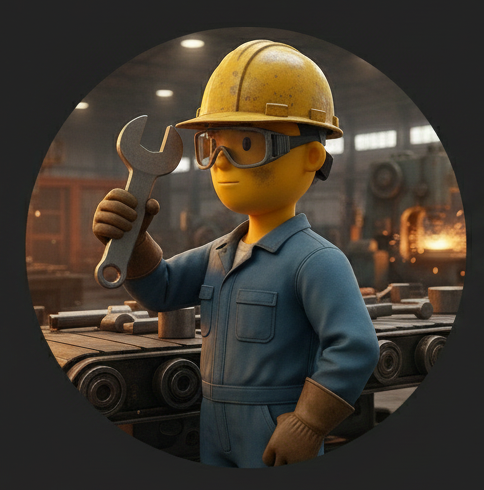
Equipment technicians maintain the complex tools that perform deposition, etching, lithography, chemical mechanical planarization (CMP), ion implantation, and metrology. Each tool type is a specialized discipline: an etch technician understands plasma physics, gas chemistry, and chamber conditioning; a lithography technician works with deep ultraviolet (DUV) and extreme ultraviolet (EUV) exposure systems that cost $150 million each; a CMP technician manages slurry chemistry, pad conditioning, and endpoint detection. Equipment maintenance combines mechanical aptitude, electrical troubleshooting, vacuum system knowledge, and chemical handling skills.
Process engineers own the recipes that define how each layer of a semiconductor device is built. They optimize deposition rates, etch selectivities, implant doses, and annealing temperatures to achieve the device specifications designed by product engineers. Yield engineers analyze defect data to identify systematic issues -- a particle source in a deposition chamber, a contamination pathway in a wet clean tool, or a lithography alignment drift -- and drive corrective actions that recover millions of dollars in product. Metrology engineers develop and maintain the measurement techniques (scanning electron microscopy, spectroscopic ellipsometry, X-ray diffraction) that verify every process step meets specification.
Salary Ranges Across Fab Roles
Clean room operators and entry-level manufacturing technicians earn $43,000 to $67,000 annually, with overtime during production ramps frequently pushing total compensation above $75,000. Semiconductor equipment technicians with 2-5 years of experience earn $47,500 to $100,000, depending on the tool specialization and fab location. Lithography and EUV technicians command the highest rates due to the complexity and cost of the equipment they maintain.
Semiconductor process engineers earn $91,000 to $130,000 or more, with specializations in etch, deposition, and lithography at the higher end. Yield engineers and integration engineers with 5-10 years of experience earn $110,000 to $150,000. Test engineers working with automated test equipment (ATE) earn $85,000 to $131,000. Fab construction roles during the current build-out phase pay $62,000 to $131,000, reflecting the urgency of the hiring need.
The CHIPS Act facilities are offering significant signing bonuses and relocation packages. Intel's Ohio fab has offered $10,000 to $30,000 signing bonuses for experienced technicians and engineers. TSMC Arizona is providing housing assistance and cross-training opportunities at its facilities in Taiwan. The competition for experienced fab workers is intense enough that salary benchmarks are moving upward 8-12% annually.
Skills-First Hiring and New Entry Pathways
The semiconductor industry is rapidly adopting skills-first hiring approaches, recognizing that the traditional pipeline of electrical engineering graduates cannot produce 115,000 new workers. AI-enabled screening tools evaluate candidates based on demonstrated competencies rather than degree requirements. Community college programs in semiconductor manufacturing technology are launching across the country, many co-developed with CHIPS Act fab operators.
Maricopa Community Colleges in Arizona partnered with TSMC to create a semiconductor technician program that feeds directly into fab operations roles. Columbus State Community College in Ohio developed a similar pathway for Intel's facilities. These programs typically run 12 to 18 months, combine classroom instruction with hands-on cleanroom experience, and lead directly to job offers starting at $45,000 to $55,000 with full benefits and tuition reimbursement for continued education.
Military veterans with electronics, avionics, or nuclear maintenance backgrounds are particularly well-suited for semiconductor manufacturing roles. The attention to procedural discipline, technical troubleshooting under pressure, and comfort with complex equipment translates directly to fab operations. Several CHIPS Act companies have established dedicated veteran hiring programs.
Advanced Packaging and the Next Frontier
Advanced packaging -- chiplet integration, system-in-package (SiP), and 3D stacking -- is the fastest-growing segment of semiconductor manufacturing. As Moore's Law scaling slows, the industry is increasingly achieving performance gains by combining multiple specialized chips in a single package rather than shrinking transistors further. This shift is creating demand for packaging engineers, bump/ball placement technicians, and reliability testing specialists -- roles that did not exist at scale five years ago.
OSAT (outsourced semiconductor assembly and test) companies like ASE, Amkor, and JCET are expanding North American operations. Intel's packaging facility in New Mexico and TSMC's advanced packaging investments in Arizona are adding thousands of positions. For technicians and engineers who specialize in advanced packaging, the combination of high demand and limited supply translates to premium compensation and rapid career advancement.
Getting Started in Semiconductor Manufacturing
The barrier to entry in semiconductor manufacturing is lower than most people assume. Fab operator positions require a high school diploma and the physical and cognitive attributes to work in a cleanroom environment. Two-year associate degree programs in semiconductor manufacturing, electronics technology, or mechatronics provide the technical foundation for equipment technician and process technician roles. Four-year degrees in electrical engineering, materials science, chemical engineering, or physics open doors to process engineering and yield engineering positions.
The current hiring environment is the most favorable in decades. With $52 billion in federal investment driving fab construction, semiconductor manufacturing is a career bet on national industrial policy. The professionals who enter the field now -- at every level from operator to engineer -- will benefit from a decade of sustained growth and investment.
Ready to connect with semiconductor manufacturers hiring in your area? Create your free profile on Automate America and get matched with fab operators, equipment manufacturers, and semiconductor companies actively recruiting for clean room and manufacturing roles.